- 打卡等级:偶尔看看III
- 打卡总天数:51
- 最近打卡:2025-10-27 08:37:58
 已绑定手机 已绑定手机 高级会员
- 积分
- 814
|
 发表于 2025-10-17 10:24:44
|
显示全部楼层
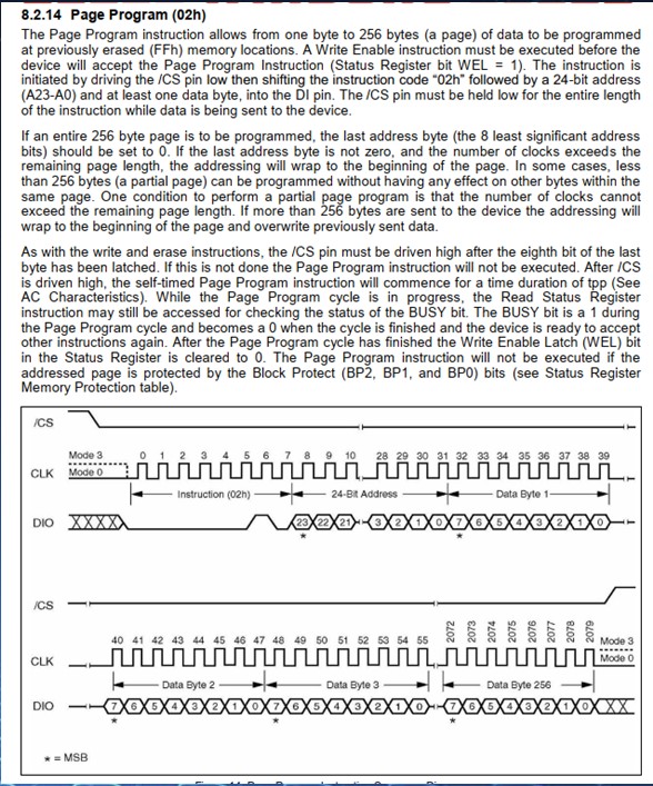
8.2.14 Page Program (02h)
The Page Program instruction allows from one byte to 256 bytes (a page) of data to be programmed at previously erased (FFh) memory locations. A Write Enable instruction must be executed before the device will accept the Page Program Instruction (Status Register bit WEL -1). The instruction is initiated by driving the /CS pin low then shifting the instruction code "02h"followed by a 24-bit address
(A23-A0) and at least one data byte, into the DI pin. The /CS pin must be held low for the entire length of the instruction while data is being sent to the device.
If an entire 256 byte page is to be programmed, the last address byte (the 8 least significant address bits) should be set to 0. If the last address byte is not zero, and the number of clocks exceeds the remaining page length, the addressing will wrap to the beginning of the page. In some cases, less than 256 bytes (a partial page) can be programmed without having any effect on other bytes within the same page. One condition to perform a partial page program is that the number of clocks cannot exceed the remaining page length. If more than 256 bytes are sent to the device the addressing will wrap to the beginning of the page and overwrite previously sent data.
As with the write and erase instructions, the /CS pin must be driven high after the eighth bit of the last byte has been latched. If this is not done the Page Program instruction will not be executed. After /CS is driven high, the self-timed Page Program instruction will commence for a time duration of tpp (See AC Characteristics). While the Page Program cycle is in progress, the Read Status Register instruction may still be accessed for checking the status of the BUSY bit. The BUSY bit is a 1 during the Page Program cycle and becomes a 0 when the cycle is finished and the device is ready to accept other instructions again. After the Page Program cycle has finished the Write Enable Latch (WEL) bit in the Status Register is cleared to 0. The Page Program instruction will not be executed if the addressed page is protected by the Block Protect (BP2, BP1, and BPO) bits (see Status Register Memory Protection table).
大致意思:
Page Program(02h)是SPI Flash操作中用于写入数据到页面的命令,其操作流程如下:操作步骤写加载(02h):发送命令02h,后跟页地址(12位)和待写入数据。数据长度为256 bytes (a page)。 1写使能(06h):发送命令06h,使能写入操作。 12写执行(10h):发送命令10h,开始写入数据到指定页面。 1状态检测:通过FSR.7轮询确认操作完成。 写入前需确保芯片处于IDLE状态,并正确配置时钟极性和相位模式。 不同厂商的扇区大小和写入时间可能不同(如Winbond扇区为1Mbit,Spansion为256Kbit)。
|
-

|
 |手机版|深圳国芯人工智能有限公司
( 粤ICP备2022108929号-2 )